

-
-
-
Cutting Plan

-

High precision cutting blades for semiconductor industry
| Blade type | Blade cutting application field | |
| Electroformed hard dicing blade | Semiconductor wafers and other silicon materials | 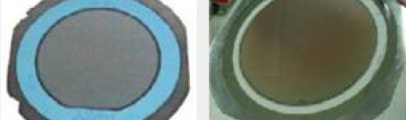 |
| Electroformed soft dicing blade | LED packaging materials, piezoelectric ceramics and other materials | 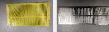 |
| Metal Blade | Integrated circuit packaging materials, ceramic materials, etc | 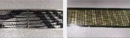 |
| Resin Blade | Integrated circuit packaging materials, superhard materials such as glass, etc | 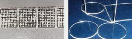 |
Application of UV cutting tape
A
Application areas of A-series products
- PCB substrate
- (BGA/QFN)
- Glass
B
Application areas of B-series products
- wafer
- MEMS
- Glass
C
Application areas of C-series products
- Ceramic
- Glass
- Crystal
V
Application areas of V series products
- wafer sawing
- Inverted film
- Expandable membrane
N
Application areas of N series products
- Non UV products
- Blue film, etc
UV film product application
PACKAGE cutting
Product model: A15010-12C、A15010-32、A15020-12C
Application process: Traditional packaging QFN, DFN, BGA and other packaging after slicing
Processing material: Epoxy resin (minimum chip size 0.6 * 0.3MM)
| Model | Base Material | Total Thickness | 180 ° Adhesion (After UV) |
| A15010-32 | PO(150μm) | 160 | 9.78(0.04) |
| A15010-12C | PO(150μm) | 160 | 15.6(0.04) |
| A15015-62H | PO(150μm) | 165 | 18.6(0.04) |
| A15020-12C | PO(150μm) | 170 | 20.3(0.05) |
MEMS product slicing
Product model: A15020-12C、A15010-12C
Application process: Wafer cutting after MEMS packaging
Processing material: epoxy resin
| Model | Base Material | Total Thickness | 180 ° adhesion (after UV) |
| A15010-12C | PO(150μm) | 170 | 15.6(0.04) |
| A15020-12C | PO(150μm) | 160 | 20.3(0.05) |
LED product slicing
Product model: A15020-32A A15010-32
Application process: After SMD and CSP packaging, chip cutting or cutting separation is required
Processing materials: EMC substrate, organic silicon, etc
| Model | Base Material | Total Thickness | 180 ° adhesion (after UV) |
| A15010-32 | PO(150μm) | 160 | 9.78(0.04) |
| A15020-12C | PO(150μm) | 170 | 18.7(0.05) |
WAFER marking
Product model: V07010-12M B09010-22D B08005-22
Application process: wafer slicing
Processing materials: WAFER
| Model | Base Material | Total Thickness | 180 ° adhesion (after UV) |
| V07010-12M | PO(150μm) | 80 | 3.52(0.04) |
| B09010--22D | PO(90μm) | 100 | 4.93(0.04) |
| B08005-22 | PO(80μm) | 85 | 7.73(0.06) |
WAFER marking
Product model: B09010-2E2A
Application process: wafer slicing
Processing materials: WAFER
| Model | Base Material | Total Thickness | 180 ° adhesion (after UV) | Anti Static |
| B09010--2E2A | PO(90μm) | 100 | 8.083(0.06) | The anti-static effect of the adhesive surface reaches 109 |

WINTIME Semiconductor Technology Co., Ltd.
Telephone:+86-513-87886889
Mobile:+86-13851530812
E-mail:shenxiangfei@ntwintime.com
Address: No. 868, Fushou East Road, Rugao City, Jiangsu Province
Quick Navigation:
Website QR code
Powered by www.300.cn | Label |